1 st Workshop “Components4Space” - ASI 2016 Peverini O. A., Addamo G., Lumia M., Virone G., Tascone R. Componenti passivi a microonde per applicazioni Spazio: Stato dell'arte e prospettive basate sull'utilizzo di tecnologie di Additive Manufacturing La Componentistica Nazionale per lo Spazio: Stato dell’arte, Sviluppi e Prospettive ASI – Roma, 18-21 Gennaio 2016 Manfredi D., Ambrosio E. P., Calignano F., Cattano G., Chiappone A., Fino P., Lorusso M., Pakkenen J., Trevisan F.
Transcript
1st Workshop “Components4Space” - ASI 2016
Peverini O. A., Addamo G., Lumia M., Virone G., Tascone R.
Componenti passivi a microonde per applicazioni Spazio:
Stato dell'arte e prospettive basate sull'utilizzo di tecnologie di Additive Manufacturing
La Componentistica Nazionale per lo Spazio: Stato dell’arte, Sviluppi e Prospettive
ASI – Roma, 18-21 Gennaio 2016
Manfredi D., Ambrosio E. P., Calignano F., Cattano G., Chiappone A., Fino P., Lorusso M., Pakkenen J., Trevisan F.
1st Workshop “Components4Space” - ASI 2016
Research Context
Expertise in RF equipment for Space
Instrumentation for scientific surveys (INAF, ASI)
Satellite communications (TAS-I - Space Antennas RF Design Unit)
Expertise in Additive Manufacturing
Robotic structures (IIT-ADVR)
Heat exchangers (PoliTo)
1st Workshop “Components4Space” - ASI 2016
Additive Manufacturing
ASTM definition of Additive Manufacturing (AM)
A process of joining materials to make objects from 3-D model data, usually layer
upon layer, as opposed to subtractive manufacturing methodologies
ASTM classification of AM technologies
Binder jetting: a liquid bonding agent is selectively deposited to join powder materials.
Direct Energy deposition: focused thermal energy is used to fuse materials by melting as they are
being deposited.
Material extrusion: material is selectively dispensed through a nozzle or orifice (Fused Deposition
Modelling)
Material jetting: droplets of build materials are selectively deposited (3-D inkjet printing)
Powder bed fusion: thermal energy selectively fuses regions of a powder bed (Electron Beam
Melting, Selective Laser Melting)
Sheet laminations: sheets of material are bonded to form an object
Vat photo-polymerization: liquid photopolymer in a vat is selectively cured by light-activated
polymerization (Stereolitography)
1st Workshop “Components4Space” - ASI 2016
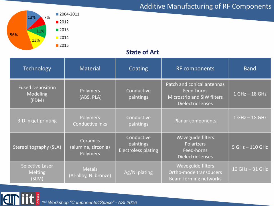
Additive Manufacturing of RF Components
Technology Material Coating RF components Band
Fused Deposition Modeling
(FDM)
Polymers (ABS, PLA)
Conductive paintings
Patch and conical antennas Feed-horns
Microstrip and SIW filters Dielectric lenses
1 GHz – 18 GHz
3-D inkjet printing Polymers
Conductive inks Conductive paintings
Planar components 1 GHz – 18 GHz
Stereolitography (SLA) Ceramics
(alumina, zirconia) Polymers
Conductive paintings
Electroless plating
Waveguide filters Polarizers
Feed-horns Dielectric lenses
5 GHz – 110 GHz
Selective Laser Melting (SLM)
Metals (Al-alloy, Ni bronze)
Ag/Ni plating Waveguide filters
Ortho-mode transducers Beam-forming networks
10 GHz – 31 GHz
State of Art
13% 7%
11%
13% 56%
2004-2011
2012
2013
2014
2015
1st Workshop “Components4Space” - ASI 2016
ESA R&D Activities in AM of RF Components
Some recent R&D activities under ESA ARTES 5.1 programme
Advanced design and manufacturing techniques for antenna feed chains
Additive manufacturing for user terminal front-ends
Miniaturised Ka-band beamforming network using additive manufacturing techniques
Some potential R&D activities under ESA GSTP-6 E.1 programme
Development of one single part integrating waveguide filter, bends, couplers, supporting structures
made by additive manufacturing
Evaluation and consolidation of additive manufacturing processes and materials for the
manufacturing of RF hardware
Development of low areal density aluminium alloy mirrors using additive manufacturing
1st Workshop “Components4Space” - ASI 2016
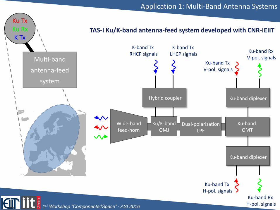
Application 1: Multi-Band Antenna Systems
Parameters Ku Tx Band Ku Rx Band K Tx Band
Operative Band (GHz) 10.7 12.75 13.0 14.5 17.7 21.2
Polarization and Versus HP&VP HP&VP LHCP/RHCP
Thermal bandwidth 35/50 MHz @ each band side
Cross Polarisation -40 dB -40 dB -40 dB
Return Loss (VSWR) -20 dB -20 dB -20 dB
Ports Isolation (any port, any band )
> 60 dB > 60 dB > 60 dB
Number of Ports 2 2 2
Waveguide WR75 WR75 WR51
Power Handling 10 carriers x
110 W (for each pol.)
N.A. 4 x 110W
(for each pol.)
Multipaction Free + 6 dB
margin N.A.
Free + 6 dB margin
Intermodulation Product Level
<-140 dBm@ (2x 120 W carriers)
Minimum IMP order 3rd 16th
TAS-I Ku/K-band antenna system for commercial SatCom
Ku Tx Ku Rx K Tx
Multi-band
antenna-feed
system
1st Workshop “Components4Space” - ASI 2016
Ku/K-band OMJ
Wide-band feed-horn
Ku-band OMT
Dual-polarization LPF
Ku-band Tx V-pol. signals
Ku-band diplexer
Ku-band Rx V-pol. signals
Ku-band diplexer
Ku-band Tx H-pol. signals
Ku-band Rx H-pol. signals
K-band Tx RHCP signals
Hybrid coupler
K-band Tx LHCP signals
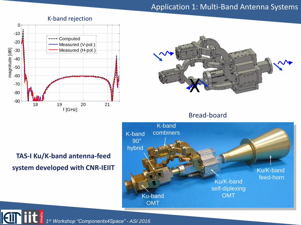
Application 1: Multi-Band Antenna Systems
TAS-I Ku/K-band antenna-feed system developed with CNR-IEIIT
Ku Tx Ku Rx K Tx
Multi-band
antenna-feed
system
1st Workshop “Components4Space” - ASI 2016
Bread-board
K-band rejection
Application 1: Multi-Band Antenna Systems
TAS-I Ku/K-band antenna-feed
system developed with CNR-IEIIT
18 19 20 21-90
-80
-70
-60
-50
-40
-30
-20
-10
0
f [GHz]
ma
gn
itud
e [
dB
]
Computed
Measured (V-pol.)
Measured (H-pol.)
Ku/K-band
feed-horn Ku/K-band
self-diplexing
OMT Ku-band
OMT
K-band
90°
hybrid
K-band
combiners
X
1st Workshop “Components4Space” - ASI 2016
Application 2: Multi-Spot SFB Antennas
Band
B1 B1 P
ola
riza
tio
n
RHCP
LHCP
Multi-spot Single-Feed per Beam (SFB)
architectures
Frequency reuse
A dedicated feed-system per each spot
(typical diameter 0.5o )
Overlapping spots
K/Ka
K/Ka
K/Ka
K/Ka
1st Workshop “Components4Space” - ASI 2016
-20 -15 -10 -5 0 5 10 15 20-20
-18
-16
-14
-12
-10
-8
-6
-4
-2
0
Theta [deg]
Ma
gn
itu
de
[d
B]
Frequency 28.0 GHz
Veq
rx TE
11
Veq
rx TM
01
Veq
rxTE
21
Ka-band OMJ
Wide-band
feed-horn K-band OMT
Dual-polarization
Ka-band SBF
K-band Tx signals
Tracking
sub-system
D-mode HF Rx signal
for tracking
High-efficiency horn
HF hybrid +
diplexers
K-band Rx signals
In-line compact assembly
Radiation patterns @ 28 GHz
Application 2: Multi-Spot SFB Antennas
K/Ka-band antenna-feed system design study
by CNR-IEIIT & TAS-I
1st Workshop “Components4Space” - ASI 2016
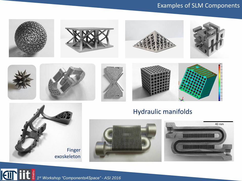
AM for Space RF Components
Advantages
Manufacturing of parts with complex geometries integration of several RF functionalities in a single block, minimization of flanges and screws (e.g. SFB and MFB SatCom systems), PIM product generation
Design flexibility novel layouts of waveguide components
Near-net shapes reduction of mass and waste
Reduction of lead time and cost more efficient component development
1st Workshop “Components4Space” - ASI 2016
AM for Space RF Components
Main concerns (?)
Manufacturing accuracy and repeatability poor RF performance @ high frequencies (Ka, Q bands)
Maximum part size no applicability to low frequency applications (C, X bands)
Surface roughness high insertion losses
Advantages
Manufacturing of parts with complex geometries integration of several RF functionalities in a single block, minimization of flanges and screws (e.g. SFB and MFB SatCom systems), PIM product generation
Design flexibility novel layouts of waveguide components
Near-net shapes reduction of mass and waste
Reduction of lead time and cost more efficient component development
1st Workshop “Components4Space” - ASI 2016
SLM Process: 3D CAD model
A set of parameters must be defined in order to respect the specifications as well as the manufacturing constraints (thicknesses, filled radii, ...).
1st Workshop “Components4Space” - ASI 2016
The main functions of the supports are to fix the part to building platform and conduct excess heat away from the part.
SLM Process: Support Structure
1st Workshop “Components4Space” - ASI 2016
A key enabling principle of AM part manufacture is the use of layers as finite 2D cross-sections of the 3D model.
SLM Process: Slicing
1st Workshop “Components4Space” - ASI 2016
SLM Process: Part Build
1st Workshop “Components4Space” - ASI 2016
SLM Process: Part Build
Technical Data
Effective building volume (including building platform)
Stress relieving by thermal treatment is used to remove residual stresses that have accumulated from manufacturing processes. The part must be separated from a build platform on which the part was produced.
SLM Process: Stress Relieving
1st Workshop “Components4Space” - ASI 2016
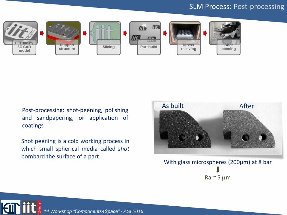
Post-processing: shot-peening, polishing and sandpapering, or application of coatings
With glass microspheres (200μm) at 8 bar
Ra ~ 5 mm
Shot peening is a cold working process in which small spherical media called shot bombard the surface of a part
SLM Process: Post-processing
After As built
1st Workshop “Components4Space” - ASI 2016
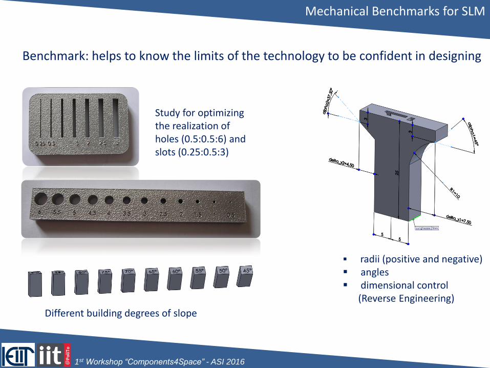
Study for optimizing the realization of holes (0.5:0.5:6) and slots (0.25:0.5:3)
Benchmark: helps to know the limits of the technology to be confident in designing
Different building degrees of slope
Mechanical Benchmarks for SLM
radii (positive and negative) angles dimensional control
(Reverse Engineering)
1st Workshop “Components4Space” - ASI 2016
Transmission coefficient
RF Benchmarks for SLM
Nominal model
ρ = 1.0E1 mW cm (typical of EDM, milling)
K-band WR51 cavity in AlSi10Mg and in Ti6Al4V
1st Workshop “Components4Space” - ASI 2016
RF Benchmarks for SLM
Nominal model
ρ = 1.0E1 mW cm (typical of EDM, milling)
DUT A
Ti6Al4V prototype “as built” ρ = 1.9E3 mW cm
Transmission coefficient
K-band WR51 cavity in AlSi10Mg and in Ti6Al4V
1st Workshop “Components4Space” - ASI 2016
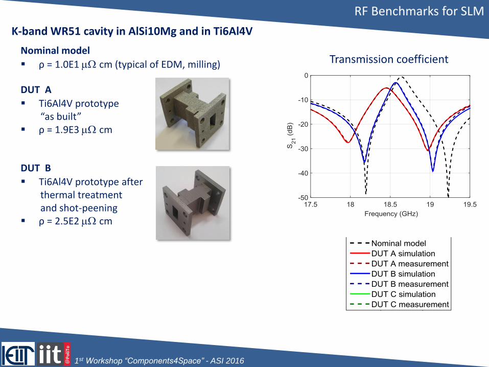
RF Benchmarks for SLM
Nominal model
ρ = 1.0E1 mW cm (typical of EDM, milling)
DUT A
Ti6Al4V prototype “as built” ρ = 1.9E3 mW cm
DUT B
Ti6Al4V prototype after thermal treatment and shot-peening ρ = 2.5E2 mW cm
Transmission coefficient
K-band WR51 cavity in AlSi10Mg and in Ti6Al4V
1st Workshop “Components4Space” - ASI 2016
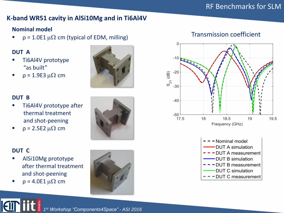
Nominal model
ρ = 1.0E1 mW cm (typical of EDM, milling)
DUT A
Ti6Al4V prototype “as built” ρ = 1.9E3 mW cm
DUT B
Ti6Al4V prototype after thermal treatment and shot-peening ρ = 2.5E2 mW cm
DUT C
AlSi10Mg prototype after thermal treatment and shot-peening ρ = 4.0E1 mW cm
RF Benchmarks for SLM
Transmission coefficient
K-band WR51 cavity in AlSi10Mg and in Ti6Al4V
1st Workshop “Components4Space” - ASI 2016
26 28 30 32 34 36 38-60
-50
-40
-30
Frequency (GHz)
Ma
gn
itu
de
(d
B)
26 28 30 32 34 36 38-0.1
-0.08
-0.06
-0.04
-0.02
0
Frequency (GHz)
Ma
gn
itu
de
(d
B)
26 28 30 32 34 36 38-70
-60
-50
-40
-30
Frequency (GHz)
Ma
gn
itu
de
(d
B) Reflection coefficient
RF Benchmarks for SLM
Ka/Q-band waveguide straights in AlSi10Mg
WR28 straights WR22 straights Ka-band circular and square straights Q-band circular and square straights
Co-polar transmission
Cross-polarization
1st Workshop “Components4Space” - ASI 2016
12 13 14 15 16
-0.25
-0.2
-0.15
-0.1
-0.05
0
Frequency (GHz)
Ma
gn
itu
de
(d
B)
Ku/K-band Low-pass Filter
Parameter Value
Pass-band 12.5 - 15.0 GHz
Stop-band 17.5 - 21.2 GHz
Return loss ≥ 24 dB
Insertion loss ≤ 0.11 dB
Rejection ≥ 40 dB
Port flange WR51
Dimension (width x height x length)
30 mm x 30 mm x 48 mm
Weight < 25 g
No tuning screws, part re-machining
or silver-plating
Insertion loss
Fifth-order WR51 stub filter in AlSi10Mg 3 prototypes
Return loss & Rejection
12 14 16 18 20 22-70
-60
-50
-40
-30
-20
-10
0
Frequency (GHz)
Ma
gn
itu
de
(d
B)
S11
S21
1st Workshop “Components4Space” - ASI 2016
12 13 14 15 16
-0.25
-0.2
-0.15
-0.1
-0.05
0
Frequency (GHz)
Ma
gn
itu
de
(d
B)
S11
S21
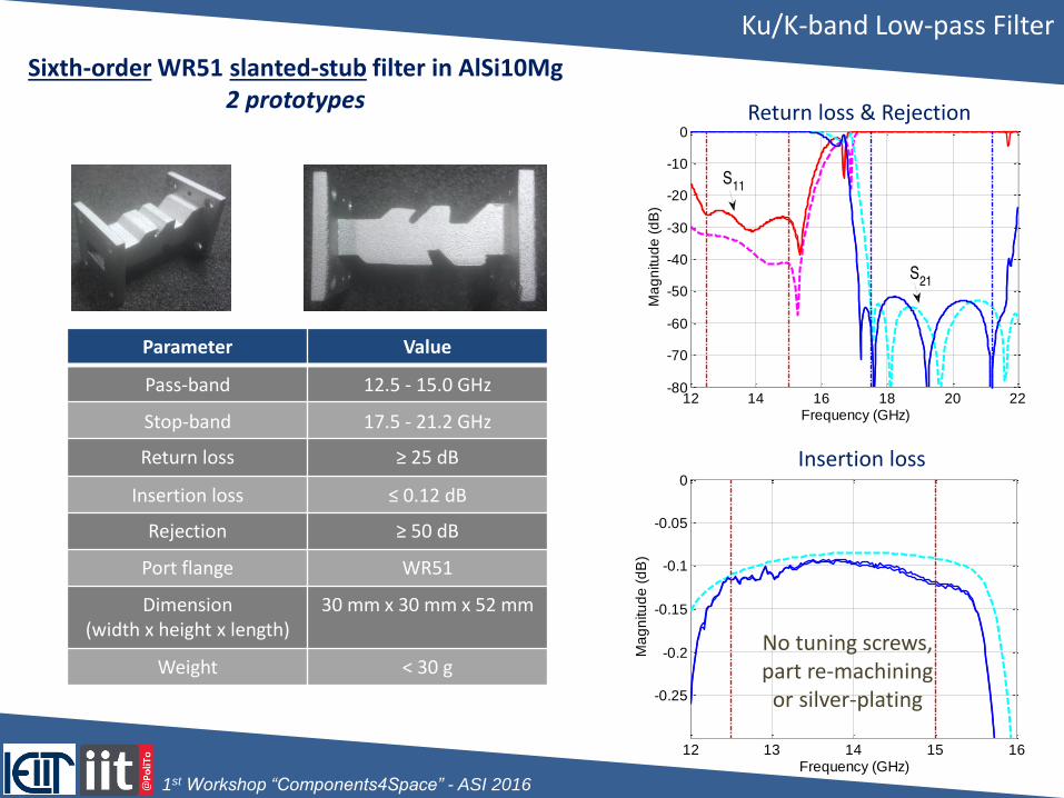
Ku/K-band Low-pass Filter
Return loss & Rejection
Parameter Value
Pass-band 12.5 - 15.0 GHz
Stop-band 17.5 - 21.2 GHz
Return loss ≥ 25 dB
Insertion loss ≤ 0.12 dB
Rejection ≥ 50 dB
Port flange WR51
Dimension (width x height x length)
30 mm x 30 mm x 52 mm
Weight < 30 g No tuning screws, part re-machining
or silver-plating
Insertion loss
Sixth-order WR51 slanted-stub filter in AlSi10Mg 2 prototypes
12 14 16 18 20 22-80
-70
-60
-50
-40
-30
-20
-10
0
Frequency (GHz)
Ma
gn
itu
de
(d
B)
S11
S21
1st Workshop “Components4Space” - ASI 2016
Conclusions
SLM manufacturing of RF components in AlSi10Mg
Mechanical accuracy: 0.1 mm (worst-case)
Surface roughness: Ra 5-15 mm
Electrical resistivity: < 16 mW cm (no coating is necessary)
Repeatability: good
Ku/K-band low-pass filters are feasible
K/Ka-band OMTs are under investigation
SLM manufacturing of RF components in Ti6Al4V
Mechanical accuracy: 0.05 mm (worst-case)
Surface roughness: Ra 4-10 mm
Electrical resistivity: > 200 mW cm (coating is necessary)
Repeatability: under investigation
Coating of complex parts is under investigation
Ku/K-band low-pass filters are under investigation
ideal for many high-performance engineering applications, for example in aerospace and motor racing, and also for the production of biomedical implants