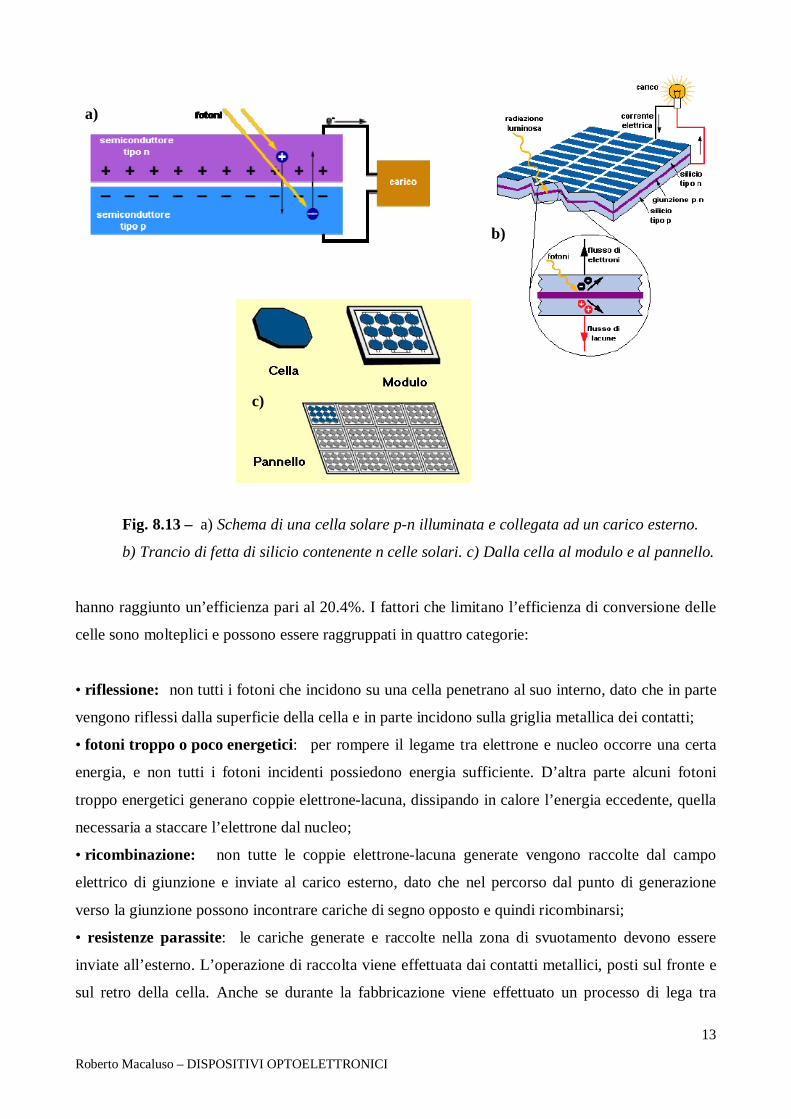
Roberto Macaluso – DISPOSITIVI OPTOELETTRONICI 12 La sensibilità del dispositivo si può regolare connettendo una resistenza variabile tra base e massa, ma abitualmente si lascia la base flottante per massimizzare la sensibilità alla luce. La contropartita di una migliore sensibilità è una minore velocità. I fototransistor sono più sensibili dei fotodiodi, ma i loro tempi di risposta sono decisamente più lenti, a causa della costante di tempo associata alla capacità e alla resistenza della regione di base. La corrente d’uscita tipica di un fotodiodo è di qualche A mentre i tempi di commutazione saturazione-interdizione sono dell’ordine di qualche ns. In un fototransistor invece, la corrente d’uscita è di qualche mA ma i tempi di commutazione sono dell’ordine dei s. 8.4 Celle solari Le celle solari sono dispositivi utili sia per applicazioni terrestri che spaziali. Esse infatti forniscono l’alimentazione di lunga durata per i satelliti e costituiscono un importante candidato per una sorgente di energia terrestre alternativa in quanto riescono a convertire direttamente la luce del sole in elettricità senza produrre alcuna forma di inquinamento ambientale. Le celle solari lavorano senza una alimentazione esterna e generano corrente e tensione convertendo potenza ottica. Illuminando con lo spettro solare una giunzione p-n si generano delle coppie elettrone-lacuna in entrambe le zone p ed n. Il campo elettrico separa gli elettroni in eccesso generati dall’assorbimento della luce, dalle rispettive lacune spingendoli in direzioni opposte (gli elettroni verso la zona n e le lacune verso la zona p). Una volta attraversata la zona svuotata di cariche libere, gli elettroni liberi non tornano più indietro, perché il campo elettrico, impedisce a loro di invertire la marcia. Se si connette la giunzione p-n attraverso un conduttore, ad un carico esterno, nel circuito così realizzato si otterrà un flusso di elettroni che parte dallo strato drogato di tipo n, a potenziale maggiore, verso lo strato p, a potenziale minore. Fino a quando la cella resta esposta alla luce, il flusso di elettroni fluirà con regolarità sotto forma di corrente continua. È importante che lo strato esposto alla luce, generalmente lo strato n, sia tale da garantire il massimo assorbimento di fotoni incidenti in vicinanza della giunzione: per il silicio questo spessore deve essere di 0,5 m, mentre lo spessore totale della cella non deve superare 0,5 mm. È chiaro che i fotoni che hanno un’energia inferiore alla banda di energia E g del silicio non generano alcuna coppia elettrone-lacuna, per cui non contribuiscono alla corrente di uscita della cella. Le figure 8.13 e 8.14 mostrano in maniera schematica il funzionamento di una cella fotovoltaica al silicio monocristallino con applicato un carico esterno. Di tutta l’energia che investe le cella solare sotto forma di radiazione luminosa, solo una parte viene convertita in energia elettrica disponibile ai suoi morsetti. L’efficienza di conversione per celle fotovoltaiche al silicio monocristallino ha raggiunto il 25%, mentre le celle al silicio policristallino
Transcript
Roberto Macaluso – DISPOSITIVI OPTOELETTRONICI
12
La sensibilità del dispositivo si può regolare connettendo una resistenza variabile tra base e
massa, ma abitualmente si lascia la base flottante per massimizzare la sensibilità alla luce.
La contropartita di una migliore sensibilità è una minore velocità. I fototransistor sono più
sensibili dei fotodiodi, ma i loro tempi di risposta sono decisamente più lenti, a causa della costante
di tempo associata alla capacità e alla resistenza della regione di base. La corrente d’uscita tipica di
un fotodiodo è di qualche A mentre i tempi di commutazione saturazione-interdizione sono
dell’ordine di qualche ns. In un fototransistor invece, la corrente d’uscita è di qualche mA ma i
tempi di commutazione sono dell’ordine dei s.
8.4 Celle solari
Le celle solari sono dispositivi utili sia per applicazioni terrestri che spaziali. Esse infatti
forniscono l’alimentazione di lunga durata per i satelliti e costituiscono un importante candidato per
una sorgente di energia terrestre alternativa in quanto riescono a convertire direttamente la luce del
sole in elettricità senza produrre alcuna forma di inquinamento ambientale. Le celle solari lavorano
senza una alimentazione esterna e generano corrente e tensione convertendo potenza ottica.
Illuminando con lo spettro solare una giunzione p-n si generano delle coppie elettrone-lacuna in
entrambe le zone p ed n. Il campo elettrico separa gli elettroni in eccesso generati dall’assorbimento
della luce, dalle rispettive lacune spingendoli in direzioni opposte (gli elettroni verso la zona n e le
lacune verso la zona p). Una volta attraversata la zona svuotata di cariche libere, gli elettroni liberi
non tornano più indietro, perché il campo elettrico, impedisce a loro di invertire la marcia.
Se si connette la giunzione p-n attraverso un conduttore, ad un carico esterno, nel circuito così
realizzato si otterrà un flusso di elettroni che parte dallo strato drogato di tipo n, a potenziale
maggiore, verso lo strato p, a potenziale minore. Fino a quando la cella resta esposta alla luce, il
flusso di elettroni fluirà con regolarità sotto forma di corrente continua.
È importante che lo strato esposto alla luce, generalmente lo strato n, sia tale da garantire il
massimo assorbimento di fotoni incidenti in vicinanza della giunzione: per il silicio questo spessore
deve essere di 0,5 m, mentre lo spessore totale della cella non deve superare 0,5 mm. È chiaro che
i fotoni che hanno un’energia inferiore alla banda di energia Eg del silicio non generano alcuna
coppia elettrone-lacuna, per cui non contribuiscono alla corrente di uscita della cella. Le figure 8.13
e 8.14 mostrano in maniera schematica il funzionamento di una cella fotovoltaica al silicio
monocristallino con applicato un carico esterno.
Di tutta l’energia che investe le cella solare sotto forma di radiazione luminosa, solo una parte viene
convertita in energia elettrica disponibile ai suoi morsetti. L’efficienza di conversione per celle
fotovoltaiche al silicio monocristallino ha raggiunto il 25%, mentre le celle al silicio policristallino
Asus
Rectangle
Asus
Typewriter
CELLE SOLARI con complementi sulle celle solari di nuova generazione
Asus
Typewriter
Asus
Typewriter
Roberto Macaluso – DISPOSITIVI OPTOELETTRONICI
13
Fig. 8.13 – a) Schema di una cella solare p-n illuminata e collegata ad un carico esterno.
b) Trancio di fetta di silicio contenente n celle solari. c) Dalla cella al modulo e al pannello.
hanno raggiunto un’efficienza pari al 20.4%. I fattori che limitano l’efficienza di conversione delle
celle sono molteplici e possono essere raggruppati in quattro categorie:
• riflessione: non tutti i fotoni che incidono su una cella penetrano al suo interno, dato che in parte
vengono riflessi dalla superficie della cella e in parte incidono sulla griglia metallica dei contatti;
• fotoni troppo o poco energetici: per rompere il legame tra elettrone e nucleo occorre una certa
energia, e non tutti i fotoni incidenti possiedono energia sufficiente. D’altra parte alcuni fotoni
troppo energetici generano coppie elettrone-lacuna, dissipando in calore l’energia eccedente, quella
necessaria a staccare l’elettrone dal nucleo;
• ricombinazione: non tutte le coppie elettrone-lacuna generate vengono raccolte dal campo
elettrico di giunzione e inviate al carico esterno, dato che nel percorso dal punto di generazione
verso la giunzione possono incontrare cariche di segno opposto e quindi ricombinarsi;
• resistenze parassite: le cariche generate e raccolte nella zona di svuotamento devono essere
inviate all’esterno. L’operazione di raccolta viene effettuata dai contatti metallici, posti sul fronte e
sul retro della cella. Anche se durante la fabbricazione viene effettuato un processo di lega tra
a)
b)
c)
Roberto Macaluso – DISPOSITIVI OPTOELETTRONICI
14
silicio e alluminio dei contatti, resta una certa resistenza all’interfaccia, che provoca una
dissipazione che riduce la potenza trasferita al carico.
Nel caso di celle al silicio policristallino, l’efficienza è ulteriormente diminuita a causa della
resistenza che gli elettroni incontrano ai confini tra un grano e l’altro.
Per aumentare la superficie attiva della cella (cioè quella che può accogliere i fotoni incidenti), la
struttura della cella viene realizzata con contatti ohmici a forma di strisce interdigitate (fig. 8.14).
Fig. 8.14 – Rappresentazione schematica di una cella p-n al silicio
Inoltre è previsto anche uno strato antiriflesso sulla superficie esposta ai raggi solari.
Per un uso pratico, le celle solari sono combinate in modo da formare un modulo fotovoltaico,
di cui sono quindi l’elemento base, mentre più moduli possono essere montati su una stessa
struttura (ad. esempio un inseguitore solare biassiale) a formare un pannello fotovoltaico (vedi fig.
8.13 c)) o vengono montate in un modulo concentratore. Quest’ultimo è un innovativo sistema
solare che consente di concentrare una grande quantità di radiazione luminosa su una piccola area di
materiale semiconduttore per generare elettricità. Diversamente dai tradizionali pannelli fotovoltaici
piani, i concentratori fotovoltaici sono spesso assai meno costosi da produrre, perché la
concentrazione permette di utilizzare un'area più piccola di celle solari, che rappresentano la parte
più costosa di un pannello fotovoltaico. Tuttavia, un costo aggiuntivo è dato dal sistema di
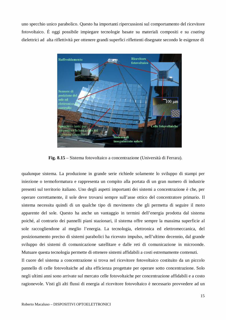
inseguimento biassiale di cui quasi tutti i concentratori necessitano. In fig. 8.15 è riportato un
esempio di sistema fotovoltaico a concentrazione. Come si può vedere, la parte più appariscente è
sicuramente il grande sistema di specchi, il concentratore primario, che ha lo scopo di concentrare
la luce proveniente dal sole sul ricevitore fotovoltaico posto nel fuoco ottico del sistema. Nel caso
rappresentato in figura, si è ricorsi ad un insieme di specchi piani per avere un’area focale
illuminata in maniera uniforme piuttosto che un punto molto luminoso come si sarebbe ottenuto con
Roberto Macaluso – DISPOSITIVI OPTOELETTRONICI
15
uno specchio unico parabolico. Questo ha importanti ripercussioni sul comportamento del ricevitore
fotovoltaico. È oggi possibile impiegare tecnologie basate su materiali compositi e su coating
dielettrici ad alta riflettività per ottenere grandi superfici riflettenti disegnate secondo le esigenze di
Fig. 8.15 – Sistema fotovoltaico a concentrazione (Università di Ferrara).
qualunque sistema. La produzione in grande serie richiede solamente lo sviluppo di stampi per
iniezione o termoformatura e rappresenta un compito alla portata di un gran numero di industrie
presenti sul territorio italiano. Uno degli aspetti importanti dei sistemi a concentrazione è che, per
operare correttamente, il sole deve trovarsi sempre sull’asse ottico del concentratore primario. Il
sistema necessita quindi di un qualche tipo di movimento che gli permetta di seguire il moto
apparente del sole. Questo ha anche un vantaggio in termini dell’energia prodotta dal sistema
poiché, al contrario dei pannelli piani stazionari, il sistema offre sempre la massima superficie al
sole raccogliendone al meglio l’energia. La tecnologia, elettronica ed elettromeccanica, del
posizionamento preciso di sistemi parabolici ha ricevuto impulso, nell’ultimo decennio, dal grande
sviluppo dei sistemi di comunicazione satellitare e dalle reti di comunicazione in microonde.
Mutuare questa tecnologia permette di ottenere sistemi affidabili a costi estremamente contenuti.
Il cuore del sistema a concentrazione si trova nel ricevitore fotovoltaico costituito da un piccolo
pannello di celle fotovoltaiche ad alta efficienza progettate per operare sotto concentrazione. Solo
negli ultimi anni sono arrivate sul mercato celle fotovoltaiche per concentrazione affidabili e a costo
ragionevole. Visti gli alti flussi di energia al ricevitore fotovoltaico è necessario provvedere ad un
Roberto Macaluso – DISPOSITIVI OPTOELETTRONICI
16
efficace sistema di raffreddamento in grado di mantenere la temperatura delle celle fotovoltaiche
sotto i 90 °C. Il problema del raffreddamento ha sempre posto un grosso ostacolo allo sviluppo di
sistemi a concentrazione ma, recentemente, problematiche simili si sono presentate nel settore
dell’elettronica professionale e dell’informatica per il raffreddamento dei microprocessori. Questo
ha spinto allo sviluppo di una tecnologia affidabile giungendo alla produzione su larga scala di
sistemi robusti e di ottime prestazioni che possono essere impiegati nei sistemi a concentrazione. Il
sistema è completato da un sensore di posizione solare e da una opportuna elettronica che controlla i
sistemi di movimento. Anche qui è oggi possibile, avvalendosi di economici microcontrollori,
sviluppare sistemi elettronici estremamente affidabili che impiegano strategie di tracciamento molto
efficaci e permettono grandi precisioni. Solo 10 anni fa un simile compito avrebbe richiesto grossi
computer con costi estremamente elevati e grossi consumi elettrici.
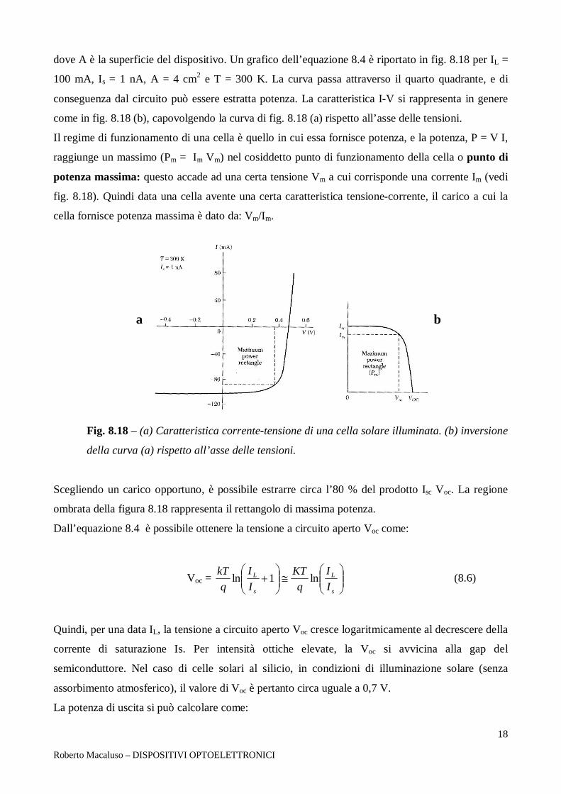
8.4.1- Caratteristica I-V delle celle solari
La cella fotovoltaica, al buio, è sostanzialmente un diodo di grande superficie. Esponendola alla
radiazione solare la cella si comporta come un generatore di corrente il cui funzionamento può
essere descritto per mezzo della caratteristica tensione-corrente come è mostrato in figura 8.16.
Se alla cella fotovoltaica non è applicato nessun carico e non vi è nessun collegamento di corto
circuito tra i contatti metallici fronte-retro, il processo fotovoltaico farà comparire ai suoi estremi
una differenza di potenziale massima di circuito aperto (open circuit) denominata Voc (in questa
Fig. 8.16 - Caratteristica I-V di una cella solare al buio e in condizioni di illuminamento.
Roberto Macaluso – DISPOSITIVI OPTOELETTRONICI
17
condizione la corrente nel dispositivo è nulla).
In condizione di corto circuito (short circuit), invece, tra il fronte e il retro della cella, si misura una
corrente massima denominata Isc con una tensione nulla agli estremi.
Quando è presente un carico esterno RL, la corrente Isc diminuisce di una quantità pari alla corrente
oscura (dark current) della cella e di direzione opposta a quella generata dal processo fotovoltaico:
questo perché con un carico esterno la cella si comporta come un diodo a cui viene applicata una
tensione, quindi nella cella oltre a generarsi una corrente per effetto fotovoltaico ci sarà anche una
corrente di diodo (dark current). In figura 8.17 è riportato il circuito equivalente (idealizzato) di una
cella solare: qui un generatore di corrente costante IL è posto in parallelo con la giunzione.
Fig. 8.17 – Schema equivalente idealizzato di una cella solare illuminata chiusa su un
carico RL.
La sorgente IL risulta dalla eccitazione delle cariche in eccesso per effetto della radiazione solare,
mentre Is è la corrente di saturazione del diodo (coincidente in questo caso con la corrente che
scorre nel diodo in condizioni di non illuminamento – dark current).
La corrente totale all’interno della cella (quella che scorre poi nel carico RL) è data dalla somma
algebrica della corrente di saturazione del diodo (Is) con la sorgente IL:
I = Is – IL (8.3)
Per un diodo ideale si ha:
I = Is (e qV/kT – 1) - IL (8.4)
e
kTEg
p
p
Dn
n
A
ss e
DN
DN
qNcNvAIJ /11
(8.5)
Asus
Rectangle
Asus
Rectangle
Asus
Rectangle
Asus
Rectangle
Asus
Typewriter
D
Asus
Typewriter
D
Asus
Typewriter
D
Roberto Macaluso – DISPOSITIVI OPTOELETTRONICI
18
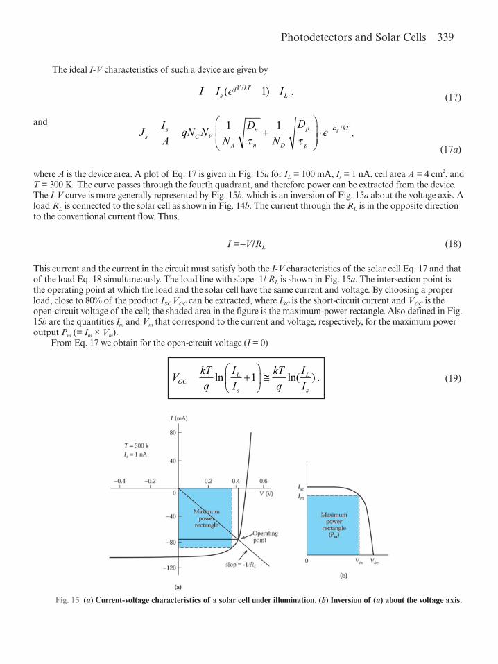
dove A è la superficie del dispositivo. Un grafico dell’equazione 8.4 è riportato in fig. 8.18 per IL =
100 mA, Is = 1 nA, A = 4 cm2 e T = 300 K. La curva passa attraverso il quarto quadrante, e di
conseguenza dal circuito può essere estratta potenza. La caratteristica I-V si rappresenta in genere
come in fig. 8.18 (b), capovolgendo la curva di fig. 8.18 (a) rispetto all’asse delle tensioni.
Il regime di funzionamento di una cella è quello in cui essa fornisce potenza, e la potenza, P = V I,
raggiunge un massimo (Pm = Im Vm) nel cosiddetto punto di funzionamento della cella o punto di
potenza massima: questo accade ad una certa tensione Vm a cui corrisponde una corrente Im (vedi
fig. 8.18). Quindi data una cella avente una certa caratteristica tensione-corrente, il carico a cui la
cella fornisce potenza massima è dato da: Vm/Im.
Fig. 8.18 – (a) Caratteristica corrente-tensione di una cella solare illuminata. (b) inversione
della curva (a) rispetto all’asse delle tensioni.
Scegliendo un carico opportuno, è possibile estrarre circa l’80 % del prodotto Isc Voc. La regione
ombrata della figura 8.18 rappresenta il rettangolo di massima potenza.
Dall’equazione 8.4 è possibile ottenere la tensione a circuito aperto Voc come:
Voc =
s
L
s
L
II
qKT
II
qkT ln1ln (8.6)
Quindi, per una data IL, la tensione a circuito aperto Voc cresce logaritmicamente al decrescere della
corrente di saturazione Is. Per intensità ottiche elevate, la Voc si avvicina alla gap del
semiconduttore. Nel caso di celle solari al silicio, in condizioni di illuminazione solare (senza
assorbimento atmosferico), il valore di Voc è pertanto circa uguale a 0,7 V.
La potenza di uscita si può calcolare come:
a b
Roberto Macaluso – DISPOSITIVI OPTOELETTRONICI
19
P = V I = Is V (eqV/kT – 1) – IL V (8.7)
La condizione per ottenere la massima potenza è ottenuta quando dP/dV = 0, ovvero:
Vm =
kTqV
qkTV
kTqVII
qkT m
ocm
sL 1ln)/(1
)/(1ln (8.8)
Im =
kTqVIe
kTqV
Im
LkTqVm
sm
/11/ (8.9)
La massima potenza Pm risulta allora:
Pm = Im Vm
qkT
kTqV
qkTVI m
ocL 1ln (8.10)
Esercizio.
Calcolare la tensione a circuito aperto e la potenza massima della cella solare di fig. 8.18 con
V = 0,35 V.
8.4.2- Efficienza di conversione
L’efficienza di conversione di potenza di una cella solare è data dal rapporto tra la potenza elettrica
massima della cella e la potenza fornita dalla luce solare incidente Pin:
η = 100in
mm
PVI
(8.11)
Un altro utile parametro delle celle solari è il fill factor (FF, fattore di riempimento), definito come:
FF = Im Vm / Isc Voc (8.12)
Esso è un indice della “quadratura” della curva I-V e indica quanto del rettangolo di massima
potenza (Im × Vm) riesce a coprire il rettangolo Isc × Voc.
L’efficienza di conversione η si può esprimere anche in funzione del fill factor FF:
η = Isc Voc FF / Pin × 100 (8.13)
Roberto Macaluso – DISPOSITIVI OPTOELETTRONICI
20
Per massimizzare l’efficienza, si dovrebbero massimizzare le tre quantità del numeratore
dell’equazione 8.13. In molte celle solari, FF ~ 70%.
La potenza di una cella fotovoltaica varia al variare della sua temperatura e della radiazione solare e
per poter fare dei confronti sono state definite delle condizioni standard di riferimento. Si è definito
in particolare il cosiddetto watt di picco (Wp) relativo alla potenza fornita dalla cella alla
temperatura di 25 °C sotto una radiazione di 1000 W/m2 e in condizioni AM = 1,51.
È importante notare, per quanto riguarda l’efficienza di conversione, che i fotoni aventi una energia
h più piccola rispetto alla gap di energia Eg del semiconduttore, non produrranno alcuna coppia
elettrone-lacuna. Inoltre, quei fotoni con energia superiore a Eg produrranno elettroni e lacune con
la stessa energia (Eg) indipendentemente da quanto grande è l’eccesso di energia (h - Eg) rispetto
ad Eg: quest’ultimo verrà semplicemente dissipato sotto forma di calore. Quindi l’efficienza di
conversione dipende criticamente da come la banda di energia del semiconduttore utilizzato si
accoppia con lo spettro di energia solare. Le celle fotovoltaiche usualmente utilizzate sono
realizzate a base di silicio, il quale presenta una lunghezza d’onda di taglio (in termini di
assorbimento) pari a 1,1 m (vedi figg. 8.19 e 8.20). Ciò significa che tutto lo spettro infrarosso non
viene interessato per la generazione di coppie elettrone-lacuna e in pratica soltanto le lunghezze
Fig. 8.19 – Irradianza spettrale della radiazione solare in condizioni di AM 0 e AM 1,5.
In figura sono indicate anche le lunghezze d’onda di taglio (cutoff) di GaAs e Si.
1 Per “air mass” (AM) si intende la massa di aria che viene attraversata dalla radiazione solare prima di incidere sulla terra. È un fattore che tiene conto quindi dell’attenuazione della luce solare per effetto delle nuvole, lo scattering e l’assorbimento atmosferico. Normalmente AM è definita come 1/cos, dove è l’angolo tra la verticale e la posizione del sole.
Roberto Macaluso – DISPOSITIVI OPTOELETTRONICI
21
d’onda comprese fra 0,55 e 0,75 m vengono catturate con efficienza quantistica superiore al 90%.
Questo implica che quasi la metà dell’energia associata allo spettro di radiazione solare non viene
convertita in energia elettrica. Un materiale che consente di ottenere efficienze di conversione
superiori al silicio è l’arseniuro di gallio (GaAs): esso ha una Eg (1,42 eV) perfettamente accoppiata
con lo spettro della radiazione solare e presenta anche un coefficiente di assorbimento superiore
rispetto a quello del silicio (vedi fig. 8.20). Questo significa che per assorbire la luce solare sono
necessari soltanto pochi m di spessore, a differenza delle celle al silicio monocristallino le quali
richiedono spessori dai 100 m in su. Infine, le celle al GaAs, a differenza di quelle al silicio,
risultano essere insensibili al calore e questo risulta un grande vantaggio specialmente in quelle
applicazioni che fanno uso di concentratori, dove le temperature raggiunte risultano abbastanza
elevate. Tipicamente, per celle al GaAs a film sottile, si raggiunge un’efficienza del 27.6 %. A
fronte di tutti questi vantaggi, bisogna dire che la tecnologia del GaAs è molto più costosa rispetto
Fig. 8.20 – Coefficiente di assorbimento dei più importanti materiali semiconduttori.
a quella del Si, per cui le celle al GaAs sono utilizzate solo per applicazioni spaziali, mentre le celle
al silicio (sia monocristallino che policristallino) sono utilizzate per applicazioni dove il costo è un
fattore chiave.
Uno dei maggiori fattori di degradazione dell’efficienza ideale di una cella solare è la resistenza
serie Rs di perdita dovuta al contatto ohmico superiore della cella. Il circuito equivalente che tiene
conto di questo effetto è riportato in fig. 8.21. L’equazione della corrente nel diodo diventa in
queste condizioni:
log [ (cm-1)]
Roberto Macaluso – DISPOSITIVI OPTOELETTRONICI
22
)(1ln ss
L IRVkTq
III
(8.14)
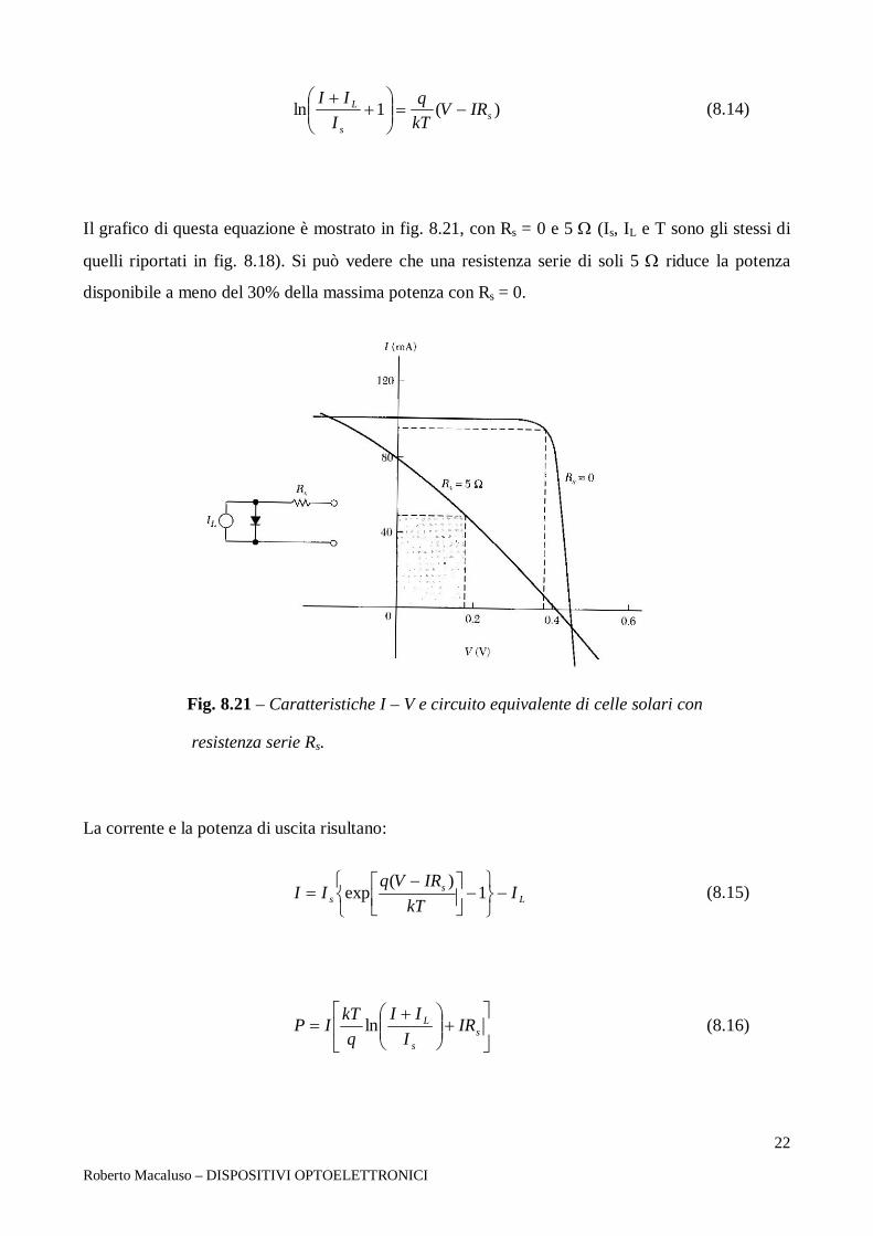
Il grafico di questa equazione è mostrato in fig. 8.21, con Rs = 0 e 5 (Is, IL e T sono gli stessi di
quelli riportati in fig. 8.18). Si può vedere che una resistenza serie di soli 5 riduce la potenza
disponibile a meno del 30% della massima potenza con Rs = 0.
Fig. 8.21 – Caratteristiche I – V e circuito equivalente di celle solari con
resistenza serie Rs.
La corrente e la potenza di uscita risultano:
Ls
s IkT
IRVqII
1)(
exp (8.15)
s
s
L IRI
IIq
kTIP ln (8.16)
Roberto Macaluso – DISPOSITIVI OPTOELETTRONICI
23
La resistenza serie dipende dalla profondità di giunzione, dalla concentrazione di impurità delle
regioni di tipo p e di tipo n e dai contatti ohmici superiori. Per una cella tipica al silicio con la
geometria mostrata in fig. 8.14, la resistenza serie è di circa 0,7 per celle n+-p e 0,4 per celle
p+-n. Questa differenza di resistenza è dovuta principalmente alla più bassa resistività nei substrati
di tipo n.
8.4.3- Stato attuale e prospettive future
Oggi, approssimativamente il 90% dei moduli fotovoltaici installati sono basati sulla tecnologia
del silicio cristallino c-Si. I principali vantaggi del silicio, che hanno contribuito al suo utilizzo
come principale materiale per applicazioni fotovoltaiche sono: il suo basso costo, la sua abbondanza
in natura, la stabilità a lungo termine e la tecnologia ben consolidata. Il principale svantaggio
associato a questa tecnologia è il prezzo troppo elevato del modulo risultante, a causa del suo alto
costo di produzione, che è la conseguenza di molti fattori:
1) il basso volume di produzione;
2) la complessità delle varie fasi del processo produttivo coinvolte nella fabbricazione della
cella e specialmente nell’assemblaggio dei moduli;
3) la richiesta di un materiale molto puro per realizzare un’alta efficienza, il quale necessita di
essere processato a temperature molto elevate e la cui sintesi chimica richiede notevoli
quantità di energia. Ogni impurità o difetto può agire come un centro di ricombinazione per
la coppia elettrone-lacuna fotogenerata, diminuendo così l’efficienza totale.
Per la fabbricazione di celle al silicio monocristallino, si utilizza silicio monocristallino ottenuto
come sottoprodotto della produzione per l’industria della microelettronica. Se si potesse avere una
produzione indipendente di silicio di grado solare, adatto cioè alla fabbricazione delle celle, allora i
costi potrebbero diminuire. Tutti questi inconvenienti, uniti al fatto che il silicio, essendo un
materiale a gap indiretta, per assicurare un assorbimento efficiente della luce solare ha bisogno di
uno strato spesso (150-300 µm), hanno incentivato lo sviluppo di nuovi approcci per ridurre il costo
delle celle fotovoltaiche. Così è stata sviluppata una seconda generazione di celle fotovoltaiche,
basata su materiali a gap diretta (tipo GaAs e InP), che permettono strati più sottili di materiale e
quindi costi più bassi. Questa tecnologia, già accennata precedentemente, viene chiamata a film
sottile (thin-film): in tal caso i materiali fotoattivi hanno uno spessore dell’ordine di pochi µm e
Roberto Macaluso – DISPOSITIVI OPTOELETTRONICI
24
sono depositati su supporti di substrato flessibili come plastica o fogli di metallo. I materiali a film
sottile usati sono: il silicio amorfo (a-Si:H) con un’efficienza pari al 10.1% , il CIGS (Copper-
Indium-Gallium-Diselenide) con un’efficienza pari al 19.6%, il CdTe (tellurio di cadmio) con
un’efficienza pari al 16.7%, misurate al NREL (National Renewable Energy Laboratory, USA).
I principali vantaggi delle celle a film sottile sono la loro leggerezza, l’utilizzo di substrati
flessibili che offrono la possibilità di un uso più versatile di questo tipo di celle rispetto alle celle
rigide del fotovoltaico convenzionale, permettendo così la loro integrazione su pareti, tetti e perfino
finestre con pannelli fotovoltaici doppi (interni ed esterni). Comunque il vantaggio principale è la
riduzione dei costi di produzione, grazie ai processi di stampa roll-to-roll, ad altissima produttività,
uguali a quelli impiegati per la stampa dei giornali.
Sebbene già con i dispositivi di seconda generazione il costo sia stato molto ridotto, non si è
ancora arrivati al punto della commercializzazione su larga scala, soprattutto a causa della
complessità produttiva del CIGS, per la sua chimica complessa, e le preoccupazioni ambientali per
quanto riguarda la tossicità del CdTe.
Nella decade passata, le tecnologie fotovoltaiche a film sottile hanno avuto un rapido sviluppo in
termini di tecnologia per la loro fabbricazione, e oggi si stanno avviando verso una rapida
espansione nella produzione industriale. I prossimi anni determineranno se questa tecnologia
porterà alla fine del dominio del mercato fotovoltaico da parte del silicio cristallino. Il tempo
necessario per una tecnologia fotovoltaica a svilupparsi da un concetto sperimentato in laboratorio
alla commercializzazione poi del prodotto è di 20 - 30 anni. Adesso che a-Si, CIGS e CdTe stanno
diventando stabili nel mercato, sorge la domanda su quale tecnologia fotovoltaica seguirà. Oggi le
ricerche procedono su due direzioni: elevata efficienza e costi di produzione bassi. Per quanto
riguarda quest’ultimo punto, sta ricevendo molta attenzione il cosiddetto fotovoltaico organico, che
include tipicamente la terza generazione di celle fotovoltaiche, le quali contengono nello strato
assorbente almeno un semiconduttore organico o una molecola organica. Le principali tecnologie
attualmente studiate, sono le celle solari tutte organiche, che comprendono le celle solari con
piccole molecole e le celle solari polimeriche, le dye-sensitized solar cells (DSSC) di Grätzel, e le
celle solari ibride che consistono in nanoparticelle inorganiche disperse in una matrice di un
polimero semiconduttore, o da maschere di semiconduttore inorganico nanostrutturato come ZnO o
TiO2 su cui sono depositati semiconduttori organici.
Altri studi sono rivolti verso soluzioni atte a massimizzare la raccolta della radiazione solare
incidente. Questo obiettivo può essere raggiunto, oltre che con i sistemi a concentrazione già
discussi precedentemente, anche attraverso lo sviluppo di celle fotovoltaiche sensibili alla
componente diffusa (es. tecnologie thin-film) e/o alle diverse componenti dello spettro solare (es.
Roberto Macaluso – DISPOSITIVI OPTOELETTRONICI
25
celle a multigiunzione) e alla ottimizzazione dei sistemi di tracking o inseguimento solare, in grado
di orientare i pannelli in maniera da massimizzare la superficie di captazione della radiazione
solare.
Fig. 11 Structures of GaAs/AlGaAs QWIPs showing approaches to coupling light to the heterointerface at a critical angle. (a) Light incident normal to a polished facet makes a 45o angle to the quantum well. (b) A grating is used to refract light coming from the substrate.1
The QWIP is an attractive alternative for long-wavelength photodetectors that use HgCdTe material, which has problems of excessive tunneling of dark current and reproducibility of the precise composition required to produce the exact energy gap. Moreover, the QWIP is compatible with GaAs technology and circuits for monolithic integration. The detection wavelength range can also be tuned by the quantum-well thickness, and the long-wavelength capability can be close to 20 μm. It has high speed and fast response due to its intrinsic short carrier lifetime in the quantum wells. One difficulty with the QWIP, at least for n-type GaAs wells, is the detection of normal-incidence light.
10.2 SOLAR CELLS
Solar cells are useful for both space and terrestrial applications. Solar cells furnish the long-duration power supply for satellites. The solar cell is an important candidate for an alternative terrestrial energy source because it converts sunlight directly to electricity with good conversion efficiency, provides nearly permanent power at low operating cost, and is virtually nonpolluting.4,5
10.2.1 Solar Radiation
The radiative energy output from the sun derives from a nuclear fusion reaction. Every second, about 6 × 10¹¹ kg hydrogen is converted to helium, with a net mass loss of about 4 × 10³ kg. The mass loss is converted through the Einstein relation (E = mc2) to 4 × 10²⁰ J. This energy is emitted primarily as electromagnetic radiation in the ultraviolet to infrared region (0.2 to 3 �m). The total mass of the sun is now about 2 × 1030 kg, and a reasonably stable life with a nearly constant radiative-energy output of over 10 billion (1010) years is projected.
The intensity of solar radiation outside the earth’s atmosphere, at the average distance of its orbit around the sun, is defined as the solar constant and has a value of 1367 W/m2. Terrestrially, the sunlight is attenuated by clouds and by atmospheric scattering and absorption. The attenuation depends primarily on the length of the light’s path through the atmosphere, or the mass of air through which it passes. This “air mass” is defined as l/cos ϕ, where ϕ is the angle between the vertical and the sun’s position.
EXAMPLE 4The air mass can most easily be estimated from the length of the shadow, s, of a vertical structure of height h, as 1
2� ( / )s h . If s = 1.118 m and h =1.00 m, find the air mass.
336 Semiconductors
Asus
Rectangle
SOLUTION
1 1 118 1 0 2 25 1 52+ ( . / . ) . . .
We have an air mass 1.5 (AM 1.5). The corresponding cos ϕ is 1/1.5 = 0.667 and the angle ϕ between the vertical and the sun’s position is cos-l (0.667) = 48o. The maximum sunlight intensity occurs when the sun is straight overhead (i.e., AM 1.0 with ϕ = 0o).
Figure 12 shows two curves related to solar spectral irradiance (power per unit area per unit wavelength).6 The upper curve, which represents the solar spectrum outside the Earth’s atmosphere, is the air mass zero condition (AM0). The AM0 spectrum is relevant for satellite and space vehicle applications. Terrestrial solar-cell performance is specified with reference to the air mass 1.5 (AM 1.5) spectrum. This spectrum represents the sunlight at the Earth’s surface when the sun is at an angle of 48o from the vertical. At this angle the incident power is about 963 W/m2.
10.2.2 p-n Junction Solar Cell
A schematic representation of a p-n junction solar cell is shown in Fig. 13. It consists of a shallow p-n junction formed on the surface, a front ohmic contact stripe and fingers, a back ohmic contact that covers the entire back surface, and an antireflection coating on the front surface. The surface reflection of the incident light from air ( n = 1) into semiconductor silicon ( n = 3.5) is about 0.31. This means that 31% of incident light is reflected and is not available for conversion to electrical energy in a silicon solar cell.
When the cell is exposed to the solar spectrum, a photon that has an energy less than the bandgap Eg makes no contribution to the cell output. A photon that has energy greater than Eg contributes an energy Eg to the cell output. Energy greater than Eg is wasted as heat. When EHPs are created in the depletion layer, they are separated by the built-in electric field. Hence, the potential difference is limited by the built-in voltage, which is in turn determined by the energy gap. On the other hand, only photons with energies larger than the bandgap are absorbed in a semiconductor, and hence the light-generated current decreases with the increase in energy gap due to the limited solar spectrum.
Fig. 12 Solar spectral irradiance6 at air mass 0 and air mass 1.5 and the cutoff wavelength of GaAs and Si.
Photodetectors and Solar Cells 337
Fig. 13 Schematic representation of a silicon p-n junction solar cell.4
To derive the conversion efficiency, we consider the energy band diagram of a p-n junction, shown in Fig. 14a, under solar radiation. We can see that VOC depends on the light intensity. The efficiency does not depend critically on the bandgap. Semiconductors with bandgaps between 1 and 2 eV can all be considered solar cell materials. The equivalent circuit is shown in Fig. 14b, where a constant-current source is in parallel with the junction. The source IL results from the excitation of excess carriers by solar radiation, Is is the diode saturation current, and RL is the load resistance.
Fig. 14 (a) Energy band diagram of a p-n junction solar cell under solar irradiation. (b) Idealized equivalent circuit of a solar cell.
338 Semiconductors
The ideal I-V characteristics of such a device are given by
I I e IsqV kT
L( ) ,/
1 (17)
and
J IA
qN NN
DN
Des
sC V
A
n
n D
p
p
E kTg+⎛
⎝⎜⎜
⎞
⎠⎟⎟⋅
1 1
τ τ/
,
(17a)
where A is the device area. A plot of Eq. 17 is given in Fig. 15a for IL = 100 mA, Is = 1 nA, cell area A = 4 cm2, and T = 300 K. The curve passes through the fourth quadrant, and therefore power can be extracted from the device. The I-V curve is more generally represented by Fig. 15b, which is an inversion of Fig. 15a about the voltage axis. A load RL is connected to the solar cell as shown in Fig. 14b. The current through the RL is in the opposite direction to the conventional current flow. Thus,
I =−V/RL (18)
This current and the current in the circuit must satisfy both the I-V characteristics of the solar cell Eq. 17 and that of the load Eq. 18 simultaneously. The load line with slope -1/ RL is shown in Fig. 15a. The intersection point is the operating point at which the load and the solar cell have the same current and voltage. By choosing a proper load, close to 80% of the product ISC VOC can be extracted, where ISC is the short-circuit current and VOC is the open-circuit voltage of the cell; the shaded area in the figure is the maximum-power rectangle. Also defined in Fig. 15b are the quantities Im and Vm that correspond to the current and voltage, respectively, for the maximum power output Pm (= Im × Vm).
From Eq. 17 we obtain for the open-circuit voltage (I = 0)
V kTq
II
kTq
IIOC
L
s
L
s
+⎛
⎝⎜
⎞
⎠⎟ ≅ln ln( ) .1 (19)
Fig. 15 (a) Current-voltage characteristics of a solar cell under illumination. (b) Inversion of (a) about the voltage axis.
Photodetectors and Solar Cells 339
Hence, for a given IL, VOC increases logarithmically with decreasing saturation current IS. The output power is given by
P IV I V e I VqV kTLs
( ) ./
1 (20)
The condition for maximum power is obtained when dP dV/ 0 , or
V kTq
I IqV kT
V kTq
qVkTm
L
mOC
m++
⎡
⎣⎢
⎤
⎦⎥ ≅ +ln
( / )
( / )ln( )
1
11
s , (21a)
I I qVkT
e IqV kTm
m qV kTL
m
m ≅⎛
⎝⎜
⎞
⎠⎟s
( )/
/1
1. (21b)
The maximum output power Pm is then
ln 1 .m
m m m L OCqVkT kTP I V I V
q kT q⎡ ⎤⎛ ⎞= ≅ − + −⎜ ⎟⎢ ⎥⎝ ⎠⎣ ⎦
(22)
EXAMPLE 5Calculate the open-circuit voltage and the output power at a voltage of 0.35 V for the solar cell shown in Fig. 15a.
SOLUTION From Eq. 19, we have
VOC×
×⎛
⎝⎜
⎞
⎠⎟( . ) ln .0 026
100 10
1 100 48
3
9V
A
AV
The output power at 0.35 V is given by Eq. 20 (note that IS and IL are reverse current so we need negative signs for them):
P e⋅ ⋅ ×( ) ( . )( ) ( . ) .. / .
10 0 35 1 0 3 48 109 0 35 0 026A V 1A) (0.35 V
22W.
10.2.3 Conversion Efficiency
Ideal efficiencyThe power conversion efficiency of a solar cell is given by
η = =
− +⎛⎝⎜
⎞⎠⎟ −
⎡
⎣⎢
⎤
⎦⎥I V
P
I V kTq
qVkT
kTq
Pm m
in
L OCm
in
ln 1 (23)
340 Semiconductors
or
η
⋅FF I VPSC OC
in
, (23a)
where Pin is the incident power and FF is the fill factor defined as
FF I VI V
kTqV
qVkT
kTqV
m m
SC OC OC
m
OC
≡ ≅ +1 1ln( ) , (24)
assuming I ISC L� . The fill factor is the ratio of the maximum power rectangle (Fig. 15b) to the rectangle of I VSC OC� . In practice, a good fill factor is around 0.8. To maximize the efficiency, we should maximize all three items in the numerator of Eq. 23a.
The ideal efficiency can be obtained from the ideal I-V characteristics defined by Eq. 17. For a given semiconductor, the saturation current density is obtained from Eq. 17a. For a given air mass condition (e.g., AM 1.5), the short-circuit current IL is the product of q and the number of the available photons with energy hν � Eg in the solar spectrum. Once IS and IL are known, the output power P and the maximum power Pm can be obtained from Eqs. 20 through 22. The input power Pin is the integration of all the photons in the solar spectrum (Fig. 12). Under AM 1.5 condition, the efficiency Pm/Pin has a broad maximum5,7 of about 29% and does not depend critically on Eg. Therefore, semiconductors with bandgap between 1 and 2 eV can all be considered as solar cell materials. Many factors degrade the ideal efficiency, so that efficiencies actually achieved are lower. The ideal peak efficiency is 31% for one sun and 37% for 1000 suns. 1,7
Spectrum Splitting The simplest way to improve the efficiency is by spectrum splitting. By splitting sunlight into narrow wavelength bands and directing each band to a cell that has a bandgap optimally chosen to convert just this band, as shown in Fig. 16a, efficiency above 60% is in principle possible.8 Fortunately, simply stacking cells on top of one another with the highest bandgap cell uppermost, as in Fig. 16b, automatically achieves an identical spectral-splitting effect, making this “tandem” cell approach a reasonably practical way of increasing cell efficiency.
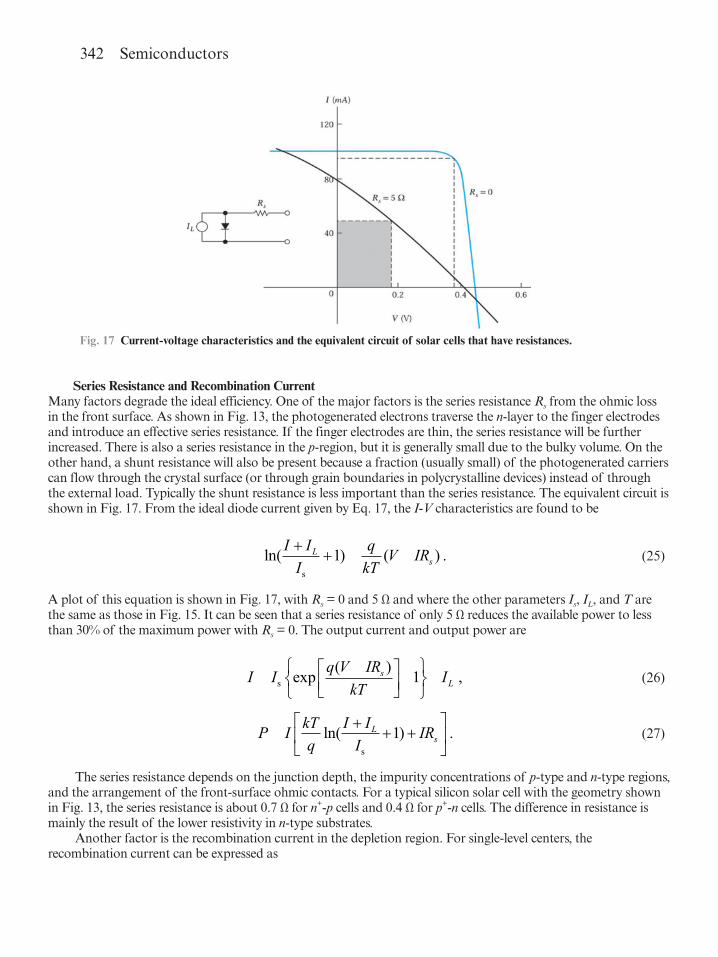
Fig. 17 Current-voltage characteristics and the equivalent circuit of solar cells that have resistances.
Series Resistance and Recombination CurrentMany factors degrade the ideal efficiency. One of the major factors is the series resistance Rs from the ohmic loss in the front surface. As shown in Fig. 13, the photogenerated electrons traverse the n-layer to the finger electrodes and introduce an effective series resistance. If the finger electrodes are thin, the series resistance will be further increased. There is also a series resistance in the p-region, but it is generally small due to the bulky volume. On the other hand, a shunt resistance will also be present because a fraction (usually small) of the photogenerated carriers can flow through the crystal surface (or through grain boundaries in polycrystalline devices) instead of through the external load. Typically the shunt resistance is less important than the series resistance. The equivalent circuit is shown in Fig. 17. From the ideal diode current given by Eq. 17, the I-V characteristics are found to be
ln( ) ( ) .I II
qkT
V IRLs
++
s
1 (25)
A plot of this equation is shown in Fig. 17, with Rs = 0 and 5 Ω and where the other parameters Is, IL, and T are the same as those in Fig. 15. It can be seen that a series resistance of only 5 Ω reduces the available power to less than 30% of the maximum power with Rs = 0. The output current and output power are
I I q V IRkT
IsL
⎡⎣⎢
⎤⎦⎥
⎧⎨⎩
⎫⎬⎭
sexp
( ),1 (26)
P I kTq
I II
IRLs
++ +
⎡
⎣⎢
⎤
⎦⎥ln( ) .
s
1 (27)
The series resistance depends on the junction depth, the impurity concentrations of p-type and n-type regions, and the arrangement of the front-surface ohmic contacts. For a typical silicon solar cell with the geometry shown in Fig. 13, the series resistance is about 0.7 Ω for n+-p cells and 0.4 Ω for p+-n cells. The difference in resistance is mainly the result of the lower resistivity in n-type substrates.
Another factor is the recombination current in the depletion region. For single-level centers, the recombination current can be expressed as
342 Semiconductors
I I qVkTrec s
⎡⎣⎢
⎤⎦⎥
'exp( ) ,
21 (28)
and
IA
qnWs i
p n
'
,
τ τ (28a)
where Is' is the saturation current. The energy conversion equation can be put into closed form to yield equations
similar to Eqs. 19 through 22, with the exception that Is is replaced by Is' and the exponential factor is divided
by 2. The efficiency for the recombination current case is found to be much less than the ideal current due to the degradation of both VOC and the fill factor. For silicon solar cells at 300 K, the recombination current can cause a 25% reduction in efficiency.
10.3 SILICON AND COMPOUND-SEMICONDUCTOR SOLAR CELLS
The main requirements for solar cells are high efficiency, low cost, and good reliability. Many solar-cell configurations have been proposed and demonstrated with impressive results. However, for solar cells to supply a significant portion of world energy, more challenges are still ahead. Nevertheless, we believe that the goal is achievable. We consider a few key solar-cell designs and their performances. In general, there are two categories of solar cells: wafer-based and thin-film solar cells.
10.3.1 Wafer-Based Solar Cells
Silicon is the most important semiconductor for solar cells. It is nontoxic and is second only to oxygen in prevalence in the earth’s crust. Therefore, silicon poses minimal environmental or resource-depletion risks if used on a large scale. It also has a well established technological base because of its use in microelectronics.
III-V compound semiconductors and their alloy systems provide wide choices of bandgaps with closely matched lattice constants. These compounds are ideal for producing tandem solar cells. For example, AlGaAs/GaAs, GaInP/GaAs, and GaInAs/InP material systems have been developed for solar cells in satellite and space vehicle applications.
Silicon PERL CellUsually, short-circuit current losses come from metal-finger coverage of the top surface, top-surface reflection loss, and imperfect light trapping in the cell. The voltage losses arise from finite surface and bulk recombination. The fill factor losses come not only from ohmic series resistance loss within the cell, but also from the same factors producing the open-circuit voltage loss. The silicon passivated emitter and rear locally-diffused (PERL) cell9 shown in Fig. 18a is a solar cell design taking all those loss factors into account.
The cell has inverted pyramids on the top that are formed by using anisotropic etches to expose the slowly etching (111) crystallographic planes. The pyramids reduce reflections of light incident on the top surface, since incident light perpendicular to the cell will strike one of the inclined (111) planes obliquely and will be refracted obliquely into the cell. This enhanced light trapping reduces the short-circuit current loss.
The cell is characterized by the use of a thin, thermally grown oxide to “passivate” (reduce the electronic activity of) the top surface of Si wafer for a junction diffusion. Then, a shallow, low-sheet-resistivity phosphorus diffusion n-layer is formed. The oxide passivation of the cell surfaces can improve the open-circuit voltage. It can also function as an antireflection coating with refractive index n = 1.46 to further reduce the total reflection. The rear locally diffused region is formed in the area of the rear point contact.
Photodetectors and Solar Cells 343
(a) (b)
Fig. 18 (a) Passivated emitter rear locally diffused (PERL) cell.9 (b) Energy-band diagram for the back-surface field.
The incorporation of a heavily doped layer under the back contact, a so-called “back-surface field,” is shown in Fig. 18b. The potential energy q p$ provides a minority carrier-reflecting region between this contact and the substrate. The back surface field also results in a very small recombination velocity at the back. Therefore, the short-circuit current will increase. The open-circuit voltage is also increased due to the increased short-circuit current. It also reduces the contact resistance and improves the fill factor. The rear contact is separated from the silicon by an intervening oxide layer. This gives much better rear reflection than an aluminum layer. To date, the PERL cell shows the highest conversion efficiency of 24.7%.
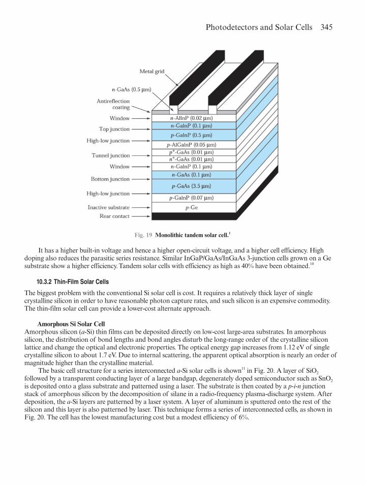
III-V Compound Tandem Solar Cell A major factor limiting conversion efficiency in single bandgap cells to 31% is that the absorbed photon energy above the semiconductor band gap is lost as heat. The main approach to reducing this efficiency loss is to use tandem p-n junctions in which higher-bandgap semiconductors and lower-bandgap semiconductors are connected together with a p+-n+ tunneling diode. Higher-energy photons are absorbed in the higher-bandgap semiconductors and lower-energy photons in the lower-bandgap semiconductors with band gaps better matched to the solar spectrum, and the overall heat loss is reduced. Stacking dozens of different cells together can theoretically increase efficiency to 68%. But this results in technical problems such as strain damages to the crystal layers. The most efficient multi-junction solar cell is one that has three cells.
Figure 19 shows the structure of a monolithic tandem solar cell.1 A p-type germanium, which has a lattice constant very close to that of GaAs and Ga0.51In0.49P, is used as the substrate. The top junction is the GaInP junction (Eg = 1.9 eV), which can absorb photons with energy hν > 1.9 eV. The bottom junction is the GaAs p-n junction (Eg = 1.42 eV), which can absorb photons with energy 1.9 eV > hν > 1.42 eV. A tunneling p+-n+ GaAs junction is placed between the top and bottom junctions to connect the cells. A p-AlGaInP layer is grown below the top junction to form a high-low junction p-AlGaInP/p-GaInP, and a p-GaInP layer is grown below the bottom junction to form a high-low junction p-GaInP/p-GaAs. They also function as a “back surface field,” as mentioned above. The potential energy barrier qϕp for the back surface field can be higher for heterojunctions than that for p-p+ homojunctions and drives minority carriers (electrons) back in the lower bandgap region of the high-low junction. There is a window at the top of each cell. A narrow layer of a wide bandgap semiconductor serves as a window, n-AlInP for the top cell and n-GaInP for the bottom cell, for the sunlight that reaches the narrow-gap semiconductor with little loss. These layers can passivate the surface defects normally present in a homojunction cell, thereby overcoming the surface recombination and improving cell efficiency. The window layer is typically very heavily doped.
344 Semiconductors
Fig. 19 Monolithic tandem solar cell.1
It has a higher built-in voltage and hence a higher open-circuit voltage, and a higher cell efficiency. High doping also reduces the parasitic series resistance. Similar InGaP/GaAs/InGaAs 3-junction cells grown on a Ge substrate show a higher efficiency. Tandem solar cells with efficiency as high as 40% have been obtained.10
10.3.2 Thin-Film Solar Cells
The biggest problem with the conventional Si solar cell is cost. It requires a relatively thick layer of single crystalline silicon in order to have reasonable photon capture rates, and such silicon is an expensive commodity. The thin-film solar cell can provide a lower-cost alternate approach.
Amorphous Si Solar CellAmorphous silicon (a-Si) thin films can be deposited directly on low-cost large-area substrates. In amorphous silicon, the distribution of bond lengths and bond angles disturb the long-range order of the crystalline silicon lattice and change the optical and electronic properties. The optical energy gap increases from 1.12 eV of single crystalline silicon to about 1.7 eV. Due to internal scattering, the apparent optical absorption is nearly an order of magnitude higher than the crystalline material.
The basic cell structure for a series interconnected a-Si solar cells is shown11 in Fig. 20. A layer of SiO2 followed by a transparent conducting layer of a large bandgap, degenerately doped semiconductor such as SnO2 is deposited onto a glass substrate and patterned using a laser. The substrate is then coated by a p-i-n junction stack of amorphous silicon by the decomposition of silane in a radio-frequency plasma-discharge system. After deposition, the a-Si layers are patterned by a laser system. A layer of aluminum is sputtered onto the rest of the silicon and this layer is also patterned by laser. This technique forms a series of interconnected cells, as shown in Fig. 20. The cell has the lowest manufacturing cost but a modest efficiency of 6%.
Photodetectors and Solar Cells 345
Fig. 20 Series-interconnected a-Si solar cells deposited on a glass substrate with a rear glass cover bonded using ethylene vinyl acetate (EVA).11
The amorphous silicon obtained by this process is incorporated with a fairly large concentration of hydrogen. The hydrogen atoms tie up dangling silicon bonds and decrease the density of localized states in the energy gap. These localized states play a dominate role in determining the carrier transport properties of amorphous silicon. The typical deposition temperature is below 300 °C, otherwise no hydrogen is incorporated in the film.
Due to the low carrier mobilities, the collection of photogenerated carriers has to be supported by an internal electrical field. To create a high field in the intrinsic layer of the p-i-n structure the cells have to be thin, of the order of a few hundred nanometers. For the p-i-n structure, the p- and n-doped layers are generally kept very thin (< 50 nm), since material quality decreases significantly as the doping level increases, and hence very few of the carriers generated in these layers contribute to photocurrent. However, these doped layers do establish an electric field in the better-quality i-layer (~ 0.5 μm thick), which aids the collection of carriers generated in this region.
In larger outdoor “power” modules, the beneficial effect of the hydrogen upon the amorphous-Si properties deteriorates under illumination. A steady drop of output efficiency occurs over the first few months. The stability problem is caused by the so called “Staebler-Wronski” degradation—the illumination by light with photon energies larger than the energy gap leads to new light-induced defect states. After that, the output stabilizes. Amorphous-Si-based modules are generally rated by manufacturers in terms of such “stabilized” output.
An improvement in efficiency can be achieved by utilizing tandem cells. High-quality a-Si:Ge:H alloys can be used as the narrow bandgap material. The bandgap of a-Si incorporated with Ge is reduced to about 1.5 eV. Therefore, we can fabricate higher efficiency a-Si:H /a-Si:Ge:H tandem cells with better collection of the red portion of the solar spectrum. A stabilized efficiency around 8% for large-area modules was obtained with these cells. A stabilized efficiency above 13% was obtained using a triple junction with the top cell consisting of a layer of a-Si:H and the bottom two cells having increased thicknesses and containing increasing percentage of germanium.5,12 But the corresponding process gas GeH4 contributes substantially to the cost of the module.
One promising microcrystalline tandem solar cell with much higher efficiency (14.5%) than the amorphous type has been developed.13,14 The structure shown in Fig. 21a consists of a microcrystalline bottom cell (μc-Si:H) and a conventional amorphous top cell in tandem. The optical energy gap of μc-Si:H is somewhere around 1 eV, which is close to that of crystalline Si and very different from that of a-Si:H (1.7 eV).
The short-wavelength light is absorbed by the top amorphous cell and long-wavelength light is absorbed by the bottom microcrystalline cell. The spectral sensitivity of the microcrystalline tandem solar cell in Fig. 21b shows higher efficiency because the microcrystalline cell absorbs the long-wavelength light that cannot be absorbed by the amorphous silicon. Compared with a-Si:H /a-Si:Ge:H tandem cells, the spectral response of the a-Si:H/μc-Si:H
346 Semiconductors
(a) (b)
Fig. 21 (a) Schematic structure and (b) typical spectral response of a microcrystalline/ amorphous tandem cell.13
tandem cell is strongly extended towards longer wavelengths. Because the microcrystalline Si has a lower optical-absorption coefficient than the amorphous type, the thickness of the i-layer of the microcrystalline solar cell needs to be much greater than the amorphous solar cell.
CIGS Solar Cell In 1974, Bell Telephone Laboratories reported the first copper indium diselenide (CuInSe2) solar cell with a conversion efficiency of 6%. In 1982, the CdS/CuInSe2 solar cell with a conversion efficiency of 10% was developed. With indium partially replaced by gallium in CuInSe2 to form the copper indium gallium diselenide (CIGS), the new material has larger optical bandgap than pure CIS, thus increasing the open-circuit voltage. The conversion efficiency of CdS/Cu(In,Ga)Se2 (CIGS) was raised to 15% in 1993, to 17.7% in 1996, to 19.2% in 2003,
5,15 and to 19.9 % in 2008.16 The CIS is a direct bandgap semiconductor material and its absorption coefficient is higher over a broader
wavelength range than other semiconductors, as shown in Fig. 22a.17 The bandgap of CIGS can vary continuously from about 1.0 eV (for CuInSe2) to about 1.7 eV (for CuGaSe2). A typical structure of CIGS solar cell is shown in Fig. 22b. The soda-lime glass [the most prevalent type of glass prepared with sodium carbonate (soda), limestone, etc.] was used as the substrate. Na ions in soda-lime glass will diffuse through Mo into CIGS during growth, and the grain of polycrystalline CIGS can grow larger with fewer defects. Sodium not only improves crystallization of the film but also increases conductivity due to the sodium incorporated at grain boundaries or defects. The mechanism is still not clear. Mo with high reflectivity and low resistivity forms good ohmic contact with CIGS. P-type CIGS absorbs most of the light and has been deposited using various methods, including co-evaporation, reactive sputtering sublimation, chemical bath deposition, laser evaporation, and spray pyrolysis. The p-n heterojunction is formed by depositing a very thin n-type CdS and an n-type transparent conducting oxide ZnO (ZnO:Al). CdS is used to modify the CIGS sensitive surface and lower the band discontinuity between ZnO and CIGS. ZnS may replace CdS due to environmental concerns. The direct deposition of ZnO on CdS will induce local defects (such as pin holes) and local fluctuations in CIGS properties (e.g., bandgap). An intrinsic ZnO (i-ZnO) buffer layer would decrease these problems. MgF2 is used as an anti-reflection coating. CIGS-based solar cells are presently one of the best candidates for a new generation of large-scale, low-cost thin-film photovoltaic systems.
Photodetectors and Solar Cells 347
(a) (b)
Fig. 22 (a) Optical absorption coefficient of CuInSe2. (b) A typical structure of CIGS solar cell.
10.4 THIRD-GENERATION SOLAR CELLS
The third generation photovoltaic cell is a range of novel alternatives to “first generation” (silicon single-crystal p-n junction or wafer solar cells) and “second generation” (low-cost, but low-efficiency thin-film) cells. Research and development in this area generally aim to provide higher efficiency and lower cost per watt of electricity generated.18
Dye-sensitized Solar CellsDye-sensitized solar cells (DSSCs) are currently the most efficient third-generation solar technology available and are ready for mass production.19 The cell in Fig. 23a has a layer of transparent conductive oxide (TCO) [usually fluorine-doped tin oxide (SnO2:F)] deposited on glass used as anode. On the conductive plate is a layer of titanium dioxide (TiO2), formed into a highly porous 3-D structure with an extremely high surface area for holding large numbers of dye molecules. The plate is then immersed in a mixture of a photosensitive ruthenium-polypyridine dye solution. The dye molecules are quite small (nanometer sized). In order to capture a reasonable amount of the incoming light, the layer of dye molecules covalently bonded on highly porous 3-D nano-structured TiO2 surface needs to be fairly thick. A separate backing is made with a thin layer of the iodide/iodine electrolyte spread over a conductive platinum sheet.
The bulk of the semiconductor (TiO2) is used solely for charge transport; the photoelectrons are provided from a separate photosensitive dye. Charge separation occurs at the surfaces between the dye, semiconductor, and electrolyte. Photons with enough energy will create an excited state of the dye, as shown in Fig. 23b. An excited electron in the conduction band has a probability to go back to valence band of the dye as the loss path 1. The excited electron can be injected directly into the conduction band of the TiO2, and from there it moves by diffusion to the anode. Meanwhile, the dye molecule strips one electron from iodide in electrolyte, oxidizing it into triiodide.
348 Semiconductors
(a)
(b)
Fig. 23 (a) DSSC cell structure. (b) Energy band diagram and main carrier losses.
This reaction occurs quite quickly compared to the time for the injected electron to recombine with the oxidized dye molecule, which is the loss path 2 shown in Fig. 23b. The triiodide then recovers its missing electron by diffusing to the counter-electrode, which reintroduces the electrons after flowing through the external circuit. The third loss is from the recombination of injected electron with the electrolyte (path 3).
Due to the porosity of the TiO2 nanostructure, there is a very high chance that a photon will be absorbed. The dye is highly efficient in converting photons into electrons, but only those electrons with enough energy can cross the TiO2 bandgap and result in photocurrent. In addition, the electrolyte limits the speed at which the dye molecules can regain their electrons and become available for photoexcitation again. These factors limit the photocurrent generated by a DSSC. The bandgap is slightly larger than silicon, which means that fewer of the photons in sunlight can be used for carrier generation. The maximum voltage generated, in theory, is simply the difference between the Fermi level of the TiO2 and the redox potential of the electrolyte, about 0.7 V (Voc). DSSCs offer slightly higher Voc than the silicon solar cell (about 0.6 V). The fill factor is about 70%, and the quantum efficiency is about 11%.20
Organic Solar CellsCarrier mobilities are very low because their transport processes are dominated by carrier hopping in organic semiconductors, as mentioned in Sec. 9.3.2 of Chapter 9, and therefore the thicknesses of organic active layers in organic solar cells are limited to a few hundred nanometers for lower series resistance. However, organic semiconductors show strong absorption in UV and visible regions and the penetration depth of the incident light is typically 80-200 nm. Thus, only a 100 nm thick organic active layer is sufficient for effective absorption. Currently, the power conversion efficiency is only 5.7 %,21 but organic solar cells attract high interest due to their large-area, low-cost potential.


![07 - LuceNaturale [modalità compatibilità] · • Valutazione energetica: UNI EN 15193 . I sistemi di griglia dovrebbero essere creati per indicare i punti in cui i valori di illuminamento](https://static.documenti.site/doc/80x56/5c67363c09d3f226588b85fb/07-lucenaturale-modalita-compatibilita-valutazione-energetica-uni.jpg)


